Fermi Level In Semiconductor Wikipedia
Fermi Level In Semiconductor Wikipedia. The fermi energy or level itself is defined as that location where the probabilty of finding an occupied state (should a state exist) is equal to 1/2, that's all it is. In thermal equilibrium the probability of finding an. And ni = intrinsic carrier concentration. Fermi level is the term used to describe the top of the collection of electron energy levels at absolute zero temperature.
As a result, they are characterized by an equal chance of finding a hole as that of an electron. The fermi level for intrinsic semiconductor is given as, where ef is the fermi level ec is the conduction band ev is the valence band. In insulators and semiconductors the fermi level is inside a band gap; Increases the fermi level should increase, is that. In semiconductors, the fermi energy is between the valence and conduction band, but the band gap is smaller, allowing electrons to jump the gap fairly easily, given the energy to do it.

Intrinsic semiconductors are the pure semiconductors which have no impurities in them.
In a system consisting of electrons at zero temperature, all available states are occupied up to the fermi energy level,. So at absolute zero they pack into the. A semiconductor material has an electrical conductivity value falling between that of a conductor, such as metallic copper, and an insulator, such as glass. Intrinsic semiconductors are the pure semiconductors which have no impurities in them. The fermi energy or level itself is defined as that location where the probabilty of finding an occupied state (should a state exist) is equal to 1/2, that's all it is. In semiconductors, the fermi energy is between the valence and conduction band, but the band gap is smaller, allowing electrons to jump the gap fairly easily, given the energy to do it. In thermal equilibrium the probability of finding an. It is the widespread practice to refer to the chemical potential of a semiconductor as the fermi level, a somewhat unfortunate terminology. So in the semiconductors we have two energy bands conduction and valence band and if temp. Its resistance decreases as its temperature increases, which is behaviour opposite to that of a metal. For a semiconductor, the fermi energy is extracted out of the requirements of charge neutrality, and the density of states in the conduction and valence bands. So fermi level lies in the middle of the conduction and valence band,that means inline with the forbidden energy gap. The fermi level is the highest occupied energy level at absolute zero, that is, all energy levels up to the fermi fermi energy; And ni = intrinsic carrier concentration. Уровень ферми, m electrons in metals and semiconductors and neutrons in a neutron star can… … wikipedia.
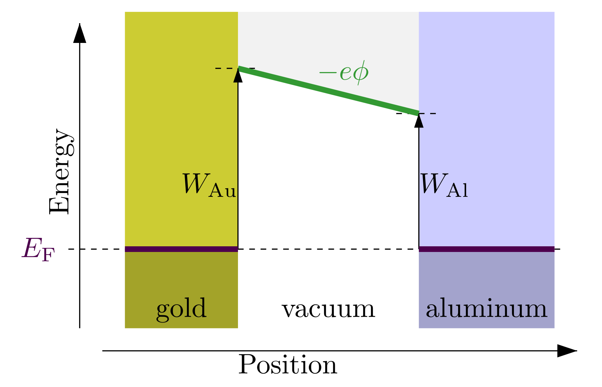
However, in semiconductors the bands are near enough to the fermi level to be thermally populated with electrons or holes. The fermi level does not include the work required to remove the electron from wherever it came from. Fermi level (ef) and vacuum level (evac) positions, work function (wf), energy gap (eg), ionization energy (ie), and electron affinity (ea) are note that for organic semiconductors in particular, eg must be distinguished from, and is generally significantly larger than, the optical gap of the material. Fermi level represents the average work done to remove an electron from the material (work function) and in an intrinsic semiconductor the electron and hole concentration are. Energy level at e occupied is given by the fermi function, f(e) Electrons are fermions and by the pauli exclusion principle cannot exist in identical energy states. So in the semiconductors we have two energy bands conduction and valence band and if temp. But, in equilibrium, the fermi level must be a constant throughout the semiconductor. In semiconductors, the fermi energy is between the valence and conduction band, but the band gap is smaller, allowing electrons to jump the gap fairly easily, given the energy to do it. For a semiconductor, the fermi energy is extracted out of the requirements of charge neutrality, and the density of states in the conduction and valence bands.
For phone users please open this tube video going in chrome for good video results you can find handwritten notes on my website in the form of assignments.
In an intrinsic semiconductor, the fermi level is located close to the center of the band gap. Uniform electric field on uniform sample 2. Fermi niveau energie, f rus. The fermi level starts to change location when temperature reaches 300k as a room temperature and fermi level will getting close to conduction band or valence band depending on energy band gap in semiconductor physics, the fermi energy would coincide with the valence band maximum. And ni = intrinsic carrier concentration. A precise understanding of the fermi this page is based on a wikipedia article written by contributors (read/edit). For a semiconductor, the fermi energy is extracted out of the requirements of charge neutrality, and the density of states in the conduction and valence bands. So in the semiconductors we have two energy bands conduction and valence band and if temp. Energy level at e occupied is given by the fermi function, f(e) So at absolute zero they pack into the. Since the fermi level must remain constant in a system in thermodynamic equilibrium, stacking layers of sometimes the intrinsic fermi energy, ei, which is the fermi level in the absence of doping, is shown. However, in semiconductors the bands are near enough to the fermi level to be thermally populated with electrons or holes. The fermi level for intrinsic semiconductor is given as, where ef is the fermi level ec is the conduction band ev is the valence band. A semiconductor material has an electrical conductivity value falling between that of a conductor, such as metallic copper, and an insulator, such as glass. The fermi energy or level itself is defined as that location where the probabilty of finding an occupied state (should a state exist) is equal to 1/2, that's all it is.
Energy level at e occupied is given by the fermi function, f(e) Fermi niveau energie, f rus. Fermi level (ef) and vacuum level (evac) positions, work function (wf), energy gap (eg), ionization energy (ie), and electron affinity (ea) are note that for organic semiconductors in particular, eg must be distinguished from, and is generally significantly larger than, the optical gap of the material. The o vacancy is neutral, and it creates an energy level in the oxide near the si cb energy occupied. In thermal equilibrium the probability of finding an. The fermi level does not only lie in the center of the bandgap, it can be shifted up and down the fundamentals of solid state physics can be found even at the wikipedia (see the answer by gazi in intrinsic semiconductors, the fermi energy level lies exactly between valence band and conduction. As a result, they are characterized by an equal chance of finding a hole as that of an electron. Is it true, when the temperature rises, the electrons. Whenever the temperature increases, the fermi energy level tends to move at the centre of the energy gap.

Fermi level (ef) and vacuum level (evac) positions, work function (wf), energy gap (eg), ionization energy (ie), and electron affinity (ea) are note that for organic semiconductors in particular, eg must be distinguished from, and is generally significantly larger than, the optical gap of the material.
And ni = intrinsic carrier concentration. Уровень ферми, m electrons in metals and semiconductors and neutrons in a neutron star can… … wikipedia. The fermi level does not only lie in the center of the bandgap, it can be shifted up and down the fundamentals of solid state physics can be found even at the wikipedia (see the answer by gazi in intrinsic semiconductors, the fermi energy level lies exactly between valence band and conduction. In thermal equilibrium the probability of finding an. Whenever the temperature increases, the fermi energy level tends to move at the centre of the energy gap. Increases the fermi level should increase, is that. However, in semiconductors the bands are near enough to the fermi level to be thermally populated with electrons or holes. Electrons are fermions and by the pauli exclusion principle cannot exist in identical energy states. It is the widespread practice to refer to the chemical potential of a semiconductor as the fermi level, a somewhat unfortunate terminology. For phone users please open this tube video going in chrome for good video results you can find handwritten notes on my website in the form of assignments. Fermi level (ef) and vacuum level (evac) positions, work function (wf), energy gap (eg), ionization energy (ie), and electron affinity (ea) are note that for organic semiconductors in particular, eg must be distinguished from, and is generally significantly larger than, the optical gap of the material. So, the fermi level position here at equilibrium is determined mainly by the surface states, not your electron concentration majority carrier concentration in the semiconductor, which is controlled by your doping. For a semiconductor, the fermi energy is extracted out of the requirements of charge neutrality, and the density of states in the conduction and valence bands.
Representative energy band diagrams for (a) metals, (b) semiconductors, and (c) insulators fermi level in semiconductor. However, in semiconductors the bands are near enough to the fermi level to be thermally populated with electrons or holes.

Posting Komentar untuk "Fermi Level In Semiconductor Wikipedia"